Silicon Carbide Enables Fast Charging Solutions - INVENTCHIP

Requirements for Modern Fast-Charging Topologies
Today’s need for fast charging solutions for electric vehicles from passenger cars up to EV trucks require highly efficient, cost-efficient topologies with a high power-density: This remains a significant challenge. According to IEC 62196 an overall efficiency η of the charging station’s power electronics of 95 to 99% is expected while the total harmonic distortion of the line current iTHD shall be lower than 8%. Additionally, the charger system including all stages of energy conversion has to be EMI compliant with the standards gathered in the series IEC 61000-4. Furthermore, a modern charger system should be able to serve different voltage levels for the battery to be charged e.g. up to 1000VDC. All these requirements ask for efficient components which enable high switching frequencies at high switching voltages.
Silicon Carbide for High Power Density
The efforts to achieve cost efficiency with high power-density create an ideal area of application for silicon carbide (SiC) based semiconductors like MOSFETs and diodes. In general, at a constant power level a higher operation voltage reduces the current and thus the needed thickness of busbars and cables. But realizing this based on silicon (Si) semiconductors like IGBTs with a higher voltage class would lead to higher conduction and switching losses. At least the switching losses could be partly compensated by reducing the switching frequency, which would significantly increase the size, weight, and cost of the magnetic components for transformers and inductors. Here MOSFETs and diodes based on silicon carbide can really make a difference. SiC MOSFETs can bring the speed of unipolar switching into voltage classes which were dominated by Si-IGBTs, while SiC diodes offer an excellent reverse-recovery behavior. Both elements based on silicon carbide additionally show a more temperature stable behavior which makes them a perfect match for topologies with a high power-density.
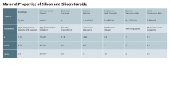
Material Properties of Si and SiC in Comparison
Table 1 shows a selection of physical properties of Silicon and Silicon Carbide* with their significance on the electrical behavior of a semiconductor. Here the factor FSiC/Si shall indicate the multiples that these parameters distinguish. Focusing on the different values for Breakdown Field Strength and the Electron Saturation Rate explains why 4H-SiC makes fast switching devices for high blocking voltages possible.
SiC Components and Driver Solutions from INVENTCHIP
INVENTCHIP Technology Co., Ltd. (abbr: IVCT) has been dedicated to developing SiC power devices, gate-drivers and controller ICs. INVENTCHIP provides customers with one-stop chip solutions focusing on SiC power semiconductor applications. They pioneered SiC MOSFET technology on 6-in wafers in China. With an automotive-grade SiC wafer fab, INVENTCHIP commits on-time and high-quality delivery of SiC products to customers and pursues continuous technology innovations. INVENTCHIP is the top SiC MOSFET provider for onboard charger applications in China. The company has sold about 51 million silicon carbide MOSFETs onto the market. In 2025 alone, more than two million EV-cars used IVCT’s silicon carbide MOSFETs, and 70% of e-compressors in China use IVCT’s gate drivers. Additionally, INVENTCHIP’s SiC semiconductors and drivers are widely used in EV chargers, photovoltaics, and energy storage applications. The reason for that is that INVENTCHIP has its own fab and can provide high quality products at a competitive price. Furthermore, INVENTCHIP supports customer designs both at the component level and at the system level.
Industry-Standard Topology for Efficient Fast-Charging Systems
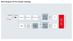
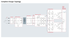
In the following, a topology is presented that is widely used across the industry. Although it is not a new design, it still shows a good balance between efficiency, power density and cost-efficiency. Figure 1 depicts the overall structure of the charger topology. Besides the required auxiliary blocks such as overvoltage- and overcurrent protection, EMI-filtering, inrush control and current measurement, the core of this topology is a Vienna Rectifier followed by two paralleled LLC bridges that feed a diode rectifier.
The outputs of these two rectifiers can be switched either in series or parallel by the voltage range selector. The last component is an ORing diode which protects the output against reverse currents and voltages. The main idea is to use one block to rectify the grid voltage. This rectified voltage feeds the LLC-inverters which provide two galvanically isolated DC-voltage sources that can be combined in series or parallel according to the needs of the battery system.
Three-Phase Vienna Rectifier in High-Power Chargers
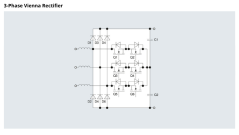
One of the core components of the charger system is the Vienna rectifier. For a high-power system, the 3-phase variant of the rectifier is used. It consists of a classical diode B6 bridge and bidirectional switches between the AC-inputs and the midpoint between the two DC-link capacitors C1 and C2. The Vienna rectifier is known to operate in Continuous Conduction Mode (CCM). It provides an inherent three-level switching and reduces the voltage stress on the switching MOSFETs. Figure 2 shows the circuit diagram of the Vienna rectifier, which combines a normal diode B6 bridge with two boost converters that share one boost inductor. For controlling the topology, hysteresis-based or carrier-based schemes are used. Equipped with 1200V-diodes and 750V-MOSFETs, it allows operation at an AC-voltage of 400VLL and provides a rectified DC-link voltage of VVienna,Out = 700-800VDC.
Operating Phases of a Rectifier Phase
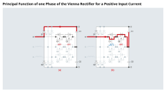
In Figure 3, only one phase is shown with its principal commutation scheme for a positive input current. In general, there are two time periods within one half-wave of the input current.
- Phase (a): The AC-current charges directly the upper DC-link capacitor C1 and magnetizes the boost inductor on the AC-side.
- Phase (b): The middle point either connects the middle point to the input node or uses the stored energy in the inductor to boost the output voltage. Here Q1 is modulated while Q2 remains switched off. For the negative half-wave, both MOSFETs alternate their functions.
Power Semiconductor Dimensioning
For the switching semiconductors, Q1-Q6 are connected to the middle point of the capacitive divider and thus only have to block half of the output DC voltage. Highly conductive SiC-MOSFETs with a low RDS(ON), like INVENTCHIP’s IV3Q07011T4Z (750V, 11mΩ) in a TO-247-4 housing, are recommended. The rectifier diodes D1-D6 must block the full DC-link voltage up to 800VDC. Therefore, the 1200V-class of SiC-diodes is recommended. INVENT-CHIP offers a wide variety of diodes in the 1200V class in most common packages. Here, the 40A types in the TO-247-2 package IV1D12040U2 or IV2D12040T2L are recommended.
Cooling and Gate Driver Design
If improved thermal performance is required and a parallel connection of the diodes is planned, two 20A types (IV1D12020T2) can be used. INVENTCHIP’s SiC diodes have a positive temperature coefficient on the forward voltage VF, which brings an inherent thermal balancing behavior in a parallel connection. In the Vienna rectifier, the electrical potentials of the gate-source-pins of the MOSFETs Q1-Q6 are floating and can’t be referenced to the control ground potential. Therefore, isolated gate drivers must be used. INVENTCHIP provides gate driver chips adapted to the special needs for the control of SiC MOSFETs. Depending on the isolation scheme of the whole converter, a high isolation voltage from primary to secondary side of the driver might be requested. IVCT’s isolated single-channel driver IVCO1412DDWQ provides an isolation voltage of up to 5.7kVRMS. For gate control, it has a maximum gate current capability of ±4A. A negative gate turn-off voltage, generated by the chip itself, avoids the risk of a parasitic turn-on while operating at high drain-source-voltage slopes dvDS/dt.
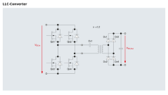
LLC Resonant Converter in the Charging System
The proposed LLC converter design consists of a standard 2L-voltage-source full bridge, which feeds a so-called LLC tank. This tank consists of a capacitor, the stray inductance as well as the main inductance of the transformer. The design of this transformer is crucial because it also provides the galvanic isolation needed for the free combination of the output voltages of the charger topology. On the secondary side of the transformer, a simple B4-diode bridge is doing the rectification of the mostly sinusoidal-shaped currents and charges the output capacitor. Figure 4 shows one LLC bridge. The voltage gain of the whole LLC topology KLLC is determined by the gain of the full bridge (= 1), the gain of the LLC tank Kres and the turn-ratio Nsec/Nprim of the transformer with KLLC = Kres ∙ Nsec/Nprim.
Design of the LLC Resonant Tank
When designing the transformer, the main inductance LM should be at least five times the stray inductance Lσ, so that the inductance ratio m = (LM + Lσ)/Lσ reaches at least 6. The main idea of this topology is to set the switching frequency of the full bridge equal to the resonant frequency fres = 1/(2π·Lσ·Cx1) of the LLC tank. In this case, the efficiency of the circuit is maximized. Switching frequencies higher than the resonant frequency will lead to an inductive behavior of the LLC load with zero-voltage switching for the MOSFETs. Switching at lower frequencies, however, leads to capacitive behavior of the load and causes additional unwanted losses in the MOSFET bridge.
Semiconductor and Driver Selection for the LLC Full Bridge
Assuming that the output voltage of the whole charging topology ranges from 300V to a maximum 1000V, and two LLC bridges are combined, a maximum DC-output voltage of VDC,out = 500V is required for one LLC bridge. Thus, with a minimum output voltage of the Vienna rectifier of 700V, the voltage gain of the LLC tank and the transformer can be defined as VDC,out / VVienna,out = KLLC = 500V / 700V = 0,71.
The semiconductors used in a MOSFET LLC full bridge must be optimized for switching rather than conduction. Therefore, IVCT’s 1200V-MOSFETs in a TO-247-4-package with a slightly higher on-state resistance IV2Q12030T4Z (with RDS(on) = 30mΩ) and IV3Q12035T4Z (with RDS(on) = 35mΩ) are recommended for the switch positions Qx1-Qx4 (x = 1, 2). The secondary diode full bridge is dimensioned for conduction. Therefore, the same diode types used in the Vienna rectifier, namely IV1D12040U2, IV2D12040T2L or two IV1D12020T2, can be used.
For the high-side switches of the MOSFET full bridge, the isolated gate driver IVCO1412DDWQ by INVENTCHIP shall be used. The low-side channels could be referenced to control ground. Therefore, non-isolated drivers like the dual (means two individual gate driver channels), non-inverting IVCR2404MPQ and the dual inverting or non-inverting IVCR2504 can be used. Both provide a maximum gate current of IG,max = ±4A.)
Conclusion and System Overview
This article presents a popular charging topology which combines efficiency of energy and cost. Figure 5 depicts the complete topology with all components. The output power is around 40kW but by using stronger components for the Vienna rectifier or a higher number of LLC stages, this outpower could be increased. It is a good solution for whether high-current or high-voltage charging. CODICO can not only supply SiC semiconductors for these charging solutions, but also support customers in selecting all necessary active and passive components for their designs, drawing on many years of expertise.
Your Contact Person
Contact Thomas Merkel for personal consultation.
